High-throughput Materials Informatics
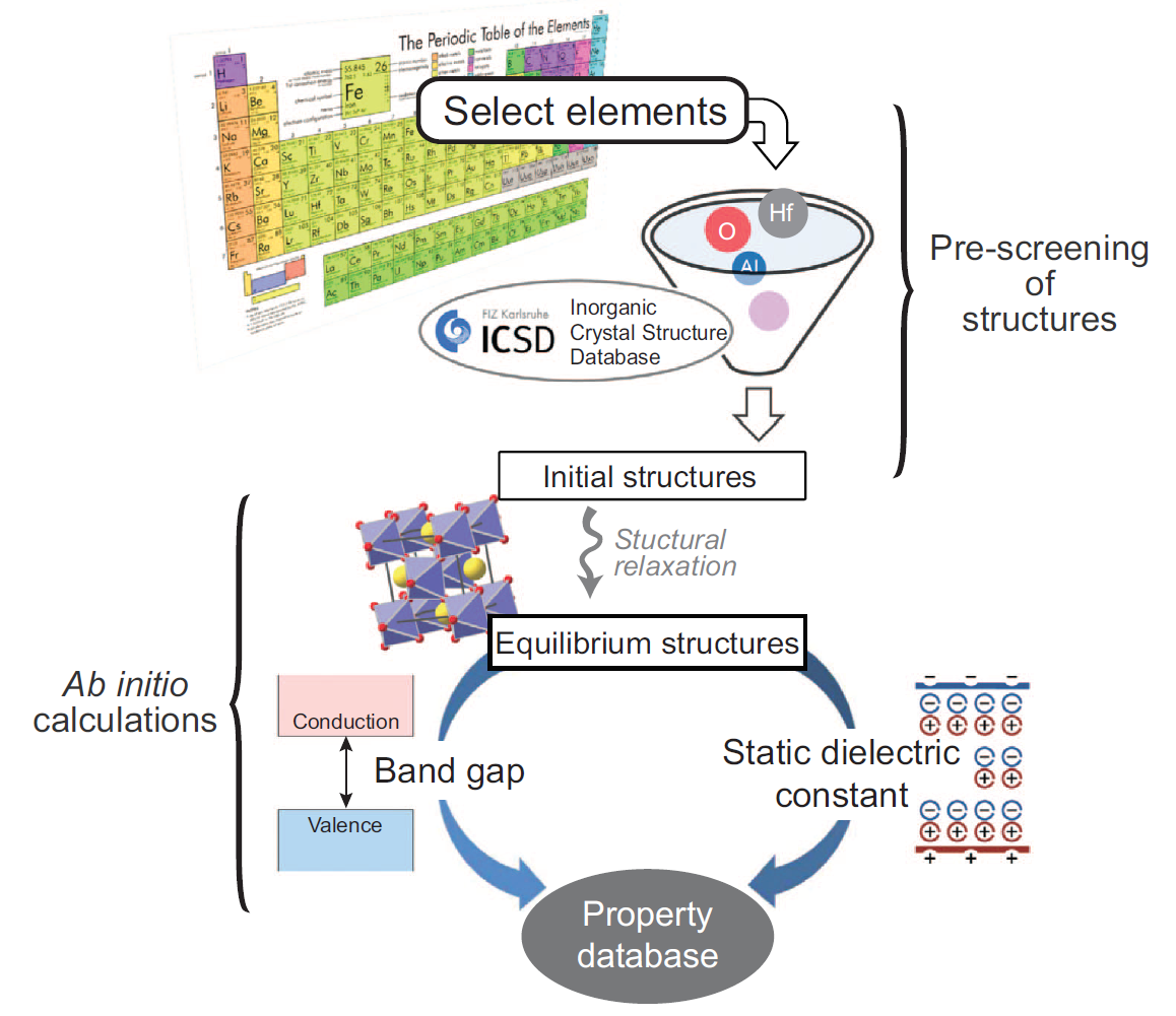
Figure 1 Schematic automation strategy to collect computational data on the band gap and static dielectric constant (Ref.: NPG Asia Mater. 7, e190 (2015))
Through the history of mankind, technical innovations of the time had always accompanied with a discovery of new material. Similarly, in modern science and technology, improving the desired properties by materials design is still the key breakthrough to overcome existing technical barriers. Even though most basic principles of material properties are well-identified by quantum mechanics during 20 century, there's still no robust way to predict the exact properties of vast unexplored materials. Recently, however, remarkable advances in computing power and first-principles calculation techniques present a new opportunity to explore this unexploited land. As the fast and accurate prediction using first-principles calculation is enabled, the high-throughput calculation is rising up as a strong tool for the data mining of materials properties.
As an example, band gap and permittivity are fundamental properties of materials and both are key properties for high-k or low-k dielectric materials for microelectronic devices. However, there are only a little portion of materials which were experimentally identified for these properties due to the costs and difficulties of the measurements. It is said that band gap and permittivity generally has trade-off relation for known materials, but there is no clear explanation about the relation and descriptors of each property are still obscure. To get the massive property database for data mining, we developed the fully-automated code (AMP2) for high-throughput calculation of band gap and static dielectric constant. As a result, we managed to calculate ~1800 binary and ternary oxide from ICSD database. From the obtained property database, we generated a materials map of the band gap versus static dielectric constant and identified new candidate materials that have not been considered in previous studies. We found some interesting candidate materials for next generation high-k dielectrics. (Ref.: NPG Asia Mater. 7, e190 (2015))
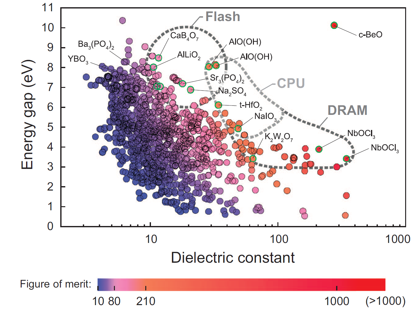
Figure 2 Eg vs κ plot for computed structures for 1158 oxides (Ref.: NPG Asia Mater. 7, e190 (2015))
Our next challenge is to find a novel p-type transparent oxide. While several n-type transparent oxides like ZnO and InGaZnO are used in consumer electronics, there are practically no p-type oxides that are comparable to the n-type counterpart. Recently, high-throughput calculation was performed to search new p-type transparent oxides, but none of candidates are validated in experiment. Thus, we tried to find a new descriptor for p-type and screened the most binary oxides using the new descriptor. Now, we are performing the high-throughput screening for ternary oxides.
2D Materials for Energy Applications
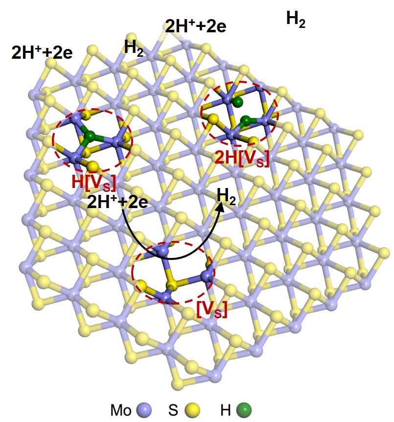
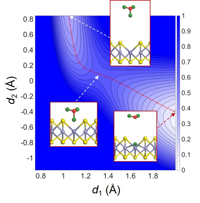
For decades, fossil fuels have been the main resource for energy production, but their reserves are limited and have a problem of CO2 and pollutants emission. One possible method to replace the fossil fuels is the hydrogen production by water splitting, particularly if it is driven by the solar energy. To obtain certain extent of efficiency, catalysts have to be placed on the surface of the electrode. For several decades, Pt is known to be the best catalyst for hydrogen evolution reaction (HER) in water splitting, but Pt is very expensive and so might not be adequate for large scale applications. As such, numerous studies searched for catalysts that have potential to replace Pt.
Recently, transition metal dichalcogenides (TMDs), most notably MoS2, are receiving much attention for water splitting because of earth abundance, stability in the acidic media, and 2D nature where the catalytic active sites might be largely exposed on the surface. However, the efficiency of TMD catalysts are not high enough to be used in practical applications. By computational approach, we are searching for new materials, mostly TMDs, that have high catalysis efficiency comparable to Pt. In addition, we explore methods to improve catalytic activity of the materials such as forming p-n junctions and applying strain by investigating electronic structures and kinetics of the reaction.
Another catalytic application of 2D materials for green environment is conversion of CO2 into useful chemicals such as CO, CH4, CH3OH, C2H4, and etc. This electrochemical reaction is first reported by Hori et al. in 1985, however, efficient catalyst that can be used in practical levels has not been discovered. By first-principles calculations, we explore possible catalysts materials that can convert CO2 into useful chemicals.
Memory Materials

 <
<
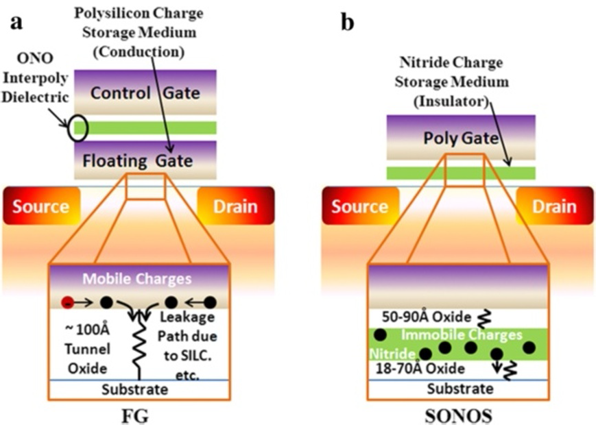
As the flash memory market has grown rapidly during the last decades, the needs to overcome the scaling limitation and the reliablity problem of the floating gate memory has been increased significantly. One of the most promising alternatives to the convential floating gate storage is the charge trap memory device in which amorphous silicon nitride (Si3N4) is utilized as the charge trapping layer. The high scalability and the retention capability originated from localized mid-gap states render the material to be a viable candidate for the memory application. It is clear that the performance of charge trap device is governed by the characteristics of the trap state, and yet the origin of the trap states is still under debate. The unclarity in the origin of the trap state comes from the amorphous nature of the charge trapping layer. The atomic configuration of amorphous Si3N4 has not been fully investigated yet because of the clear resolution limit of experimental tools. Therefore, computer-aided theoretical methods are indispensable in understanding amorphous materials.
We carry out first-principles calculations to generate amorphous ensembles using melt-quench protocol within density functional theory (DFT) molecular dynamics. Each structure is optimized with hybrid functional method in which the description of energetics and electronic structure is superior to conventional DFT. The atomic configuration of the trap states is analyzed and the effect of the trap configuration on the charge state level is discussed. This study will give a useful insight into designing and optimizing the charge trap devices based on amorphous Si3N4.
Organic Electronics : Multiscale Simulation Study
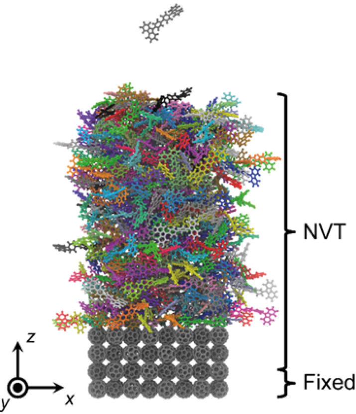
Recently, it has been reported that controlling molecular orientation in vapor-deposited organic film can play a prominent role in determining the performance of organic optoelectronic devices. Although the experiment unveils that the particular molecular ordering leads to higher outcoupling efficiency and charge carrier mobility, a rigorous understanding of the relationship between the film morphology and the device performance is still lacking. In this regard, we performed a series of computer simulations to elucidate how the morphology of organic films can affect hole transport phenomena in hole-only devices. Molecular dynamic simulations were adopted to build organic films of different structural disorder which govern the details of transport parameters. In the following step, the charge hopping rate is calculated based on semi-classical Marcus theory where reorganization energy, electronic coupling, and distribution of energies of hopping sites are taken into account via ab-initio calculation and molecular dynamics using polarizable force fields. Finally, kinetic Monte Carlo algorithm is employed to compute the charge carrier mobility for the given film structure in the course of process of charge hopping event. Our results indicate that the films deposited below glass transition temperature show higher spatial autocorrelation in site energy as well as higher charge carrier mobility than those of the films deposited above glass transition temperature, which in turn highlights the importance of processing.
Neural Network Based Potentials

The density functional theory (DFT) calculations are widely used in materials research, both in basic and industrial applications. While the DFT calculation provides highly accurate information about material properties, its application is still limited to a few pico-seconds molecular dynamics (MD) simulations with several hundred atoms. With classical force fields, one can handle much larger systems up to million atoms and several nanoseconds. However, the accuracy of classical MD simulations critically depends on the interatomic potentials. Although several classical potentials are poised be accurate and transferable the number of the classical force field is still limited and optimizing the parameters in the force field requires strenuous efforts.
Recently, neural network (NN) based potential are gaining much attention. The NN potential is constructed through the machine learning on the reference ab initio data. Since NNs can provide efficient and promising models for the arbitrary functional forms between given atomic coordinates and its potential energy surface, it gives interatomic potential that shows accuracy comparable to DFT. However, the optimal way to train the NN potential is still unknown and the reliability of the NN potential is questionable.
We developed SNU neural network atomic potential package (SNAPP) which can be used for data preprocessing, neural network training and NN potential MD simulations (LAMMPS implemented). We are currently working finding a optimal method to train defective systems such as point defects surfaces and interfaces. We are also working on developing an indicator which gives a warning sign when the MD simulation is likely to fail.
Facility
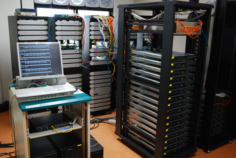
Computing System
Loki

4 nodes :
2 * Intel(R) Xeon(R) CPU E5-2650 2.00GHz
4 * 20MB cache memory
64GB RAM
(Installed date : 2013.02)
4 * 20MB cache memory
64GB RAM
(Installed date : 2013.02)
4 nodes :
2 * Intel(R) Xeon(R) CPU E5-2670 2.60GHz
4 * 20MB cache memory
128GB RAM
(Installed date : 2013.08)
4 * 20MB cache memory
128GB RAM
(Installed date : 2013.08)
4 nodes :
2 * Intel(R) Xeon(R) CPU E5-2680V2 2.80GHz
4 * 20MB cache memory
64GB RAM
(Installed date : 2014.04)
4 * 20MB cache memory
64GB RAM
(Installed date : 2014.04)
Athena
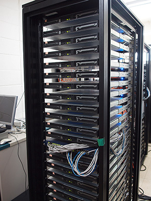
24 nodes :
2 * Intel(R) Xeon(R) CPU E5520 2.27GHz
4 * 8MB cache memory
32GB RAM
(Installed date : 2009)
4 * 8MB cache memory
32GB RAM
(Installed date : 2009)

8 nodes :
2 * Intel(R) Xeon(R) CPU E5-2630 2.30GHz
4 * 16MB cache memory
64GB RAM
(Installed date : 2012.5)
4 * 16MB cache memory
64GB RAM
(Installed date : 2012.5)
Enki

24 nodes :
2 * Intel(R) Xeon(R) E5420 2.50GHz
6MB cache memory
12GB RAM
(Installed date : 2006)
6MB cache memory
12GB RAM
(Installed date : 2006)


