Plasma MEMS DEVICE
Atmospheric plasma technology has been much of interest due to its versatile usages, such as air pollution control and analytic spectroscopy. Advantage of atmospheric plasma technology includes simplicity of plasma generation by eliminating a vacuum pump. But it is very hard to sustain stable atmospheric plasma due to arc transition and a high operating voltage. HMED investigates feasibility of micro-machined electrodes as atmospheric plasma generating device. Using MEMS technology, an array of precisely controlled micron gaps can be fabricated and it reduces a bias voltage required for plasma generation substantially. Stable atmospheric plasma has been successfully demonstrated at 250 V using an array of the microelectrode (JVST. B 2007, JJAP 2009).
Nano FET
Source/Drain Design for 16 nm Surrounding Gate MOSFETs
A gate-last MOSFET has been suggested for 32 nm node CMOSFET, where the integration of a high-k gate dielectric and a metal gate electrode becomes essential to meet the transistor performance requirement. The gate-last MOSFET has been demonstrated as an effective integration scheme to avoid thermal instability and workfunction mismatch issues.
We investigate an optimized S/D design for gate structures that had been reported for a 16 nm MOSFET. The high-k surrounding MOSFET is found to achieve comparable delay to the conventional gate structure, but the minimum delay is obtained with an underlap S/D, which is in contrary to the conventional one with an overlap S/D. It is also found that more underlap is preferred for the high-k surrounding gate MOSFET as the permittivity of the gate dielectric layer increases.
Organic Thin-Film Transistors
The general contention that organic thin-film transistors (OTFTs) represent a potential Low-cost alternative to their silicon counterpart for large area and flexible electronics has propelled intense research activities in recent years.
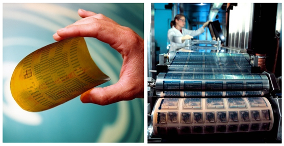
.Fig.1 Organic Thin-film Transistors on plastic substrate *source: Phillps, Poly IC
-DC characteristics of OTFTs-
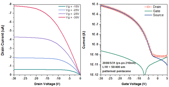
Current – Voltage measurements are a convenient method for DC-characterizing OTFTs. (Fig.2)When evaluating the electrical characteristics of OTFTs, the parameters most often calculated and reported are the field-effect mobility, on/off current ratio, subthreshold slope and Threshold voltage. These parameters ate extracted from the output characteristics (Id-Vd) and transfer characteristics (Id-Vg). (Fig.3)
Fig.2 Cross section view of OTFT and schematic of DC measurements/Conventional material for OTFTs

-AC characteristics of OTFTs-
A lot work in literature has been reported on the characterization and modeling of the DC-characteristic of OTFTs but only limited work has been reported on the AC-characteristics. In the design of analog circuits these AC-characteristic play a very important role. To enable the further development of organic circuits the characterization and modeling of these dynamic properties will be essential.Capacitance-Voltage and Capacitance-Frequency measurement provide important information on the nature of the dielectric/semiconductor interface and dynamic behavior of OTFTs. HMED has to extract the division of the gate capacitance in a gate-source and a gate-drain part of OTFTs for the AC-modeling and limitation of contact region and overlap capacitance has been studied using MIS (Metal-Insulator-Semiconductor) structure .Furthermore, trap state in bulk and interface (trap and release) and fixed charge of different dielectric are suggested.
국가
대한민국
소속기관
홍익대학교 (학교)
연락처
책임자
김영민 ymkim@wow.hongik.ac.kr


